![]() This work is licensed under a Creative Commons Attribution 4.0 International License.
This work is licensed under a Creative Commons Attribution 4.0 International License.
Following the research on Kerr frequency combs.

![]() This work is licensed under a Creative Commons Attribution 4.0 International License.
This work is licensed under a Creative Commons Attribution 4.0 International License.
You must be logged in to post a comment.
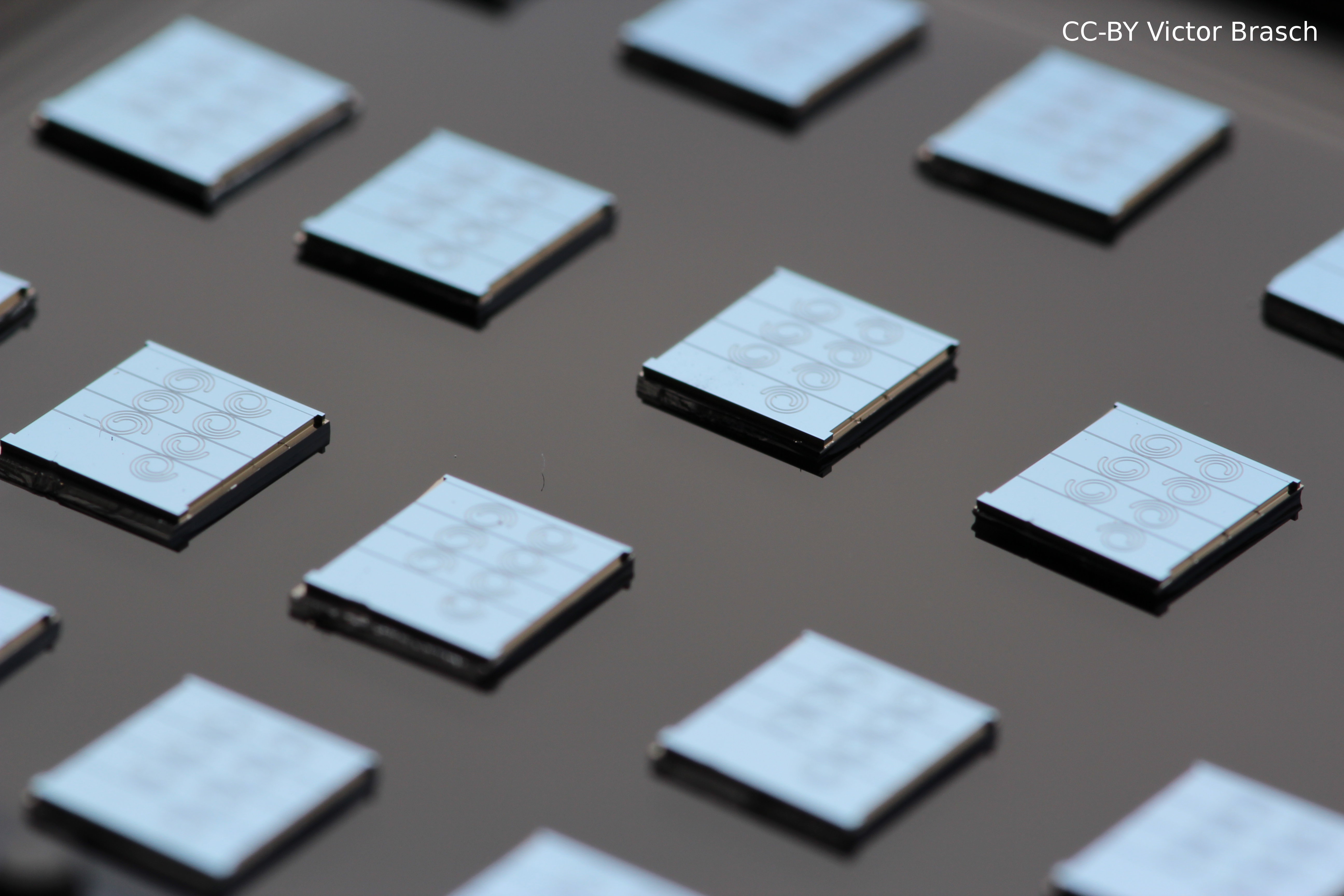
Can I ask how these chips diced? or how do you define the edges of the chips? e.g. optical lithography? or dicing saw?
Sure. So, the picture is a bit older. By that time we used to define the facets/edges of the chips with optical lithography and etch around 200µm deep into the silicon wafer and then break/cleave the remaining ~300µm of the wafer. This resulted in the very well defined, etched upper part including the facets where we couple light in and out and the somewhat less well defined pedestal below. The two parts are also visible on the photograph. These days we still etch our chips and the facets but we do not break the wafer anymore.